Buried Junction Box Defects
by Claire Kearns-McCoy & Michael Scott
This article was originally published in pv magazine - July/August 2026 Edition.
Claire Kearns-McCoy and Michael Scott of Intertek CEA report a rise in junction box failures across utility-scale and rooftop solar sites – from performance-robbing solder defects to outright fires – and explain why the only reliable window to catch these problems closes as soon as the potting compound cures.
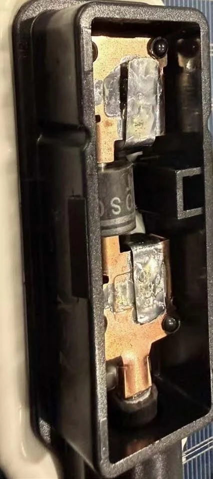
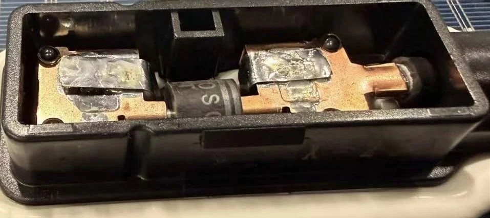
A junction box terminal with a partial solder joint was sufficient for the module to pass a flash test but will cause performance loss over a longer period.
Early signs of junction box (JB) failure are often subtle. It may be an infrared signature detected during a commissioning- stage drone flyover, or a technician noting cracking in the JB cover of an otherwise normal looking module. Left unaddressed, one failure may progress to a fire.
This is a growing concern. Junction box failures now rank among the most common problems Intertek CEA’s field team investigates, and defect rates on sites can be as high as 10% of installed modules.
Three distinct failure modes drive these events: poor soldering of the busbar ribbon to the junction box terminal, failed soldering of the bypass diode inside the junction box, and degraded or improperly applied adhesive or potting compound that allows moisture into the module. All three trace back to the factory, and they become undetectable once the potting compound cures and seals the junction box interior. However, each is preventable with the right checks at the right stage.
Failure modes
The most common failure starts with the busbar ribbon. After lamination, conductive ribbons that pass through the module backsheet or rear glass must be bent vertically for junction box installation. Workers or automated processes affix the junction box then bend the ribbons back down onto the terminals where they are soldered.
A ribbon that is not fully seated on the terminal produces a poor connection with limited cross-sectional area. Under the brief burst of a factory flash test, that marginal contact carries enough current to make a normal IV curve, but under continuous field illumination, it acts as a resistor, generating heat that can eventually cause a thermal event in the junction box. There will not be an external sign of a defect as it lies buried under the potting compound.
The industry-wide switch to half-cell modules as standard increases risk. Where a full-cell module from 10 years ago had a single junction box, today’s half-cell modules are equipped with up to three, multiplying the number of solder joints per panel that can experience this failure mode.
A marginal connection that passes the flash test may not fail immediately. As the module heats and cools through daily thermal cycling, small mechanical stresses accumulate. A joint that makes barely adequate contact on day one can fail completely after a short time in the field, taking a whole substring or diode offline.
The second failure mode involves the bypass diode. Each diode sits dormant during normal operation, so a failed solder connection between the diode and its terminal causes no measurable performance loss until a cell substring gets shaded. At that point, instead of the diode rerouting current around the shaded cells, those cells must absorb current from the rest of the string in reverse causing severe heat inside the module laminate.
Like the ribbon-to-terminal defect, a failed diode solder joint can pass a flash test and remain invisible once the potting cures. It also tends to take longer to manifest, because the diode only activates under partial shading and therefore sees fewer thermal cycles before the marginal solder joint degrades.
The third failure mode – degraded or improperly applied adhesive and potting – has become more common over the last few years. This is seen most often at newer, less experienced factories, particularly when buyers have selected on price. Junction box adhesive must squeeze out evenly around the perimeter when the box presses onto the backsheet. That squeeze-out confirms adequate coverage.
If manufacturers apply too little adhesive to reduce cleanup labor, coverage gaps can let moisture reach the terminals. The potting compound itself mixes from two parts. If the ratio is wrong, expired or incorrectly mixed potting can fail to cure properly.
Factory fault
“The top three causes of junction box failure
■ Poor soldering of the busbar
■ Failed soldering of the bypass diode
■ Degraded or poorly applied adhesive or potting compound”
The only reliable in-factory inspection window for ribbon-to-terminal solder quality is before potting cures. Pre-shipment inspection is inadequate, because even if the junction box lid is removed, the potting covers the joints. Some suppliers use translucent potting, but the limited visibility makes the defects difficult to detect. The only place to reliably catch a marginal solder connection is inline, during production, while the terminal surface is accessible.
There are two approaches to consider. Automated optical inspection (AOI) when cameras compare each solder joint against a library of acceptable and defective images, flagging anything that deviates for human review. AOI can flag shape anomalies, but it images the surface of a silver solder blob, which varies enough in appearance that marginal joints slip through.
Physical probing is more reliable. This involves a technician pressing each ribbon onto the terminal with a metal probe to confirm the joint holds under mechanical force. A ribbon that is not fully seated will move.
In the United States, where factory labor costs run significantly higher than some other regions, and turnover remains a challenge, the probing step gets skipped or understaffed more often. When an Intertek CEA factory inspection team finds a quality problem during inline monitoring, the finding goes back to the module buyer. This often produces results faster than any internal factory quality program, as customers can use findings as leverage in the procurement process – requiring corrective action.
The better long-term solution is to improve welding technology. Replacing conventional silver blob with laser welding results in discrete, precisely defined weld spots that optical inspection can evaluate clearly. Each spot passes or fails. Factories installing new production lines should specify laser welding. Those running existing conventional equipment rarely upgrade in advance, as most wait for a breakdown, but the case for laser welding on any new line is straightforward.
In the field
Most junction box solder failures surface within the first year of operation, making commissioning- stage or routine operational infrared (IR) scanning an effective first catch. The IR signature of a failing ribbon-to-terminal joint and the IR signature of a module with severe microcracks can look identical – both can produce a substring that is in open circuit.
That matters for warranty claims. Module manufacturers will often attribute the finding to storm damage, mishandling, or improper installation. Root cause analysis that rules out mechanical damage and demonstrates the manufacturing origin puts the liability where it belongs.
Warranty claims for confirmed junction box defects generally succeed, but a successful warranty claim does not eliminate the cost of labor to replace modules, the logistical burden of managing replacements, or the downtime. Spare inventory often gets depleted on sites with high failure rates, requiring new modules to be shipped from the factory.
Claire Kearns-McCoy is a senior engineering manager at Intertek CEA. She has 12 years of PV experience, including extensive work conducting field testing and interpreting test results. Kearns-McCoy has participated in projects including electroluminescence imaging and analysis for over 55,000 PV modules. She previously worked at SunEdison in solar module research, development, and manufacturing management for solar wafers, cells and modules.
Michael Scott is a senior quality control engineer with Intertek CEA. He has more than 23 years of experience in solar, ranging from academic research to high volume manufacturing. Before joining Intertek CEA, Scott worked in several highly technical engineering and leadership positions at SunPower Corporation and SolarWorld. Before his work in silicon PV manufacturing, Scott studied third-generation thinfilm PV technologies in graduate school and professional research.